


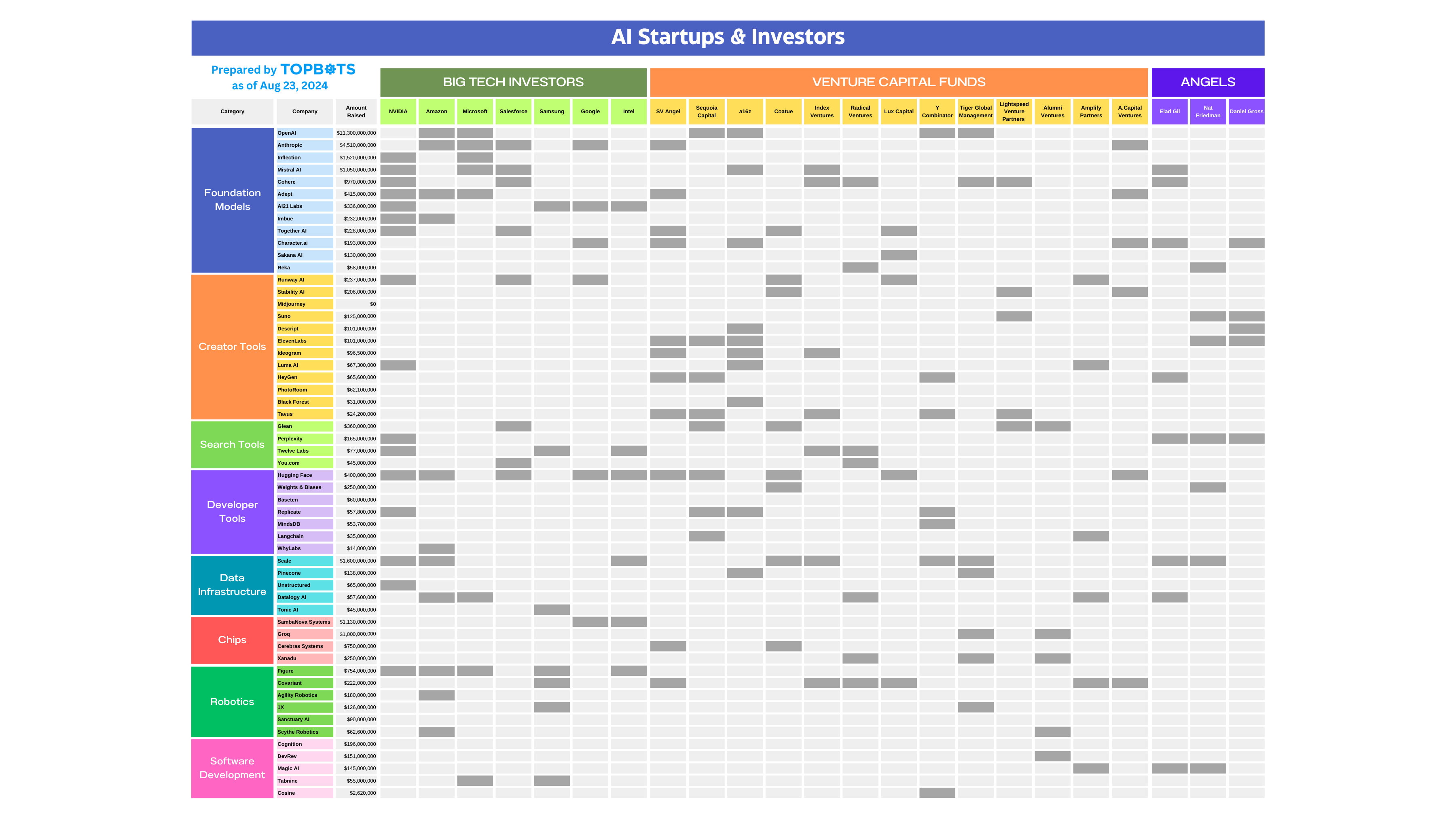
![[The AI Show Episode 151]: Anthropic CEO: AI Will Destroy 50% of Entry-Level Jobs, Veo 3’s Scary Lifelike Videos, Meta Aims to Fully Automate Ads & Perplexity’s Burning Cash](https://www.marketingaiinstitute.com/hubfs/ep%20151%20cover.png)


_Suriya_Phosri_Alamy.jpg?width=1280&auto=webp&quality=80&disable=upscale#)


![Epic Games: Apple’s attempt to pause App Store antitrust order fails [U]](https://i0.wp.com/9to5mac.com/wp-content/uploads/sites/6/2025/05/epic-games-app-store.jpg?resize=1200%2C628&quality=82&strip=all&ssl=1)


![Does the Galaxy Watch 8 ‘squircle’ design appeal to you? [Poll]](https://i0.wp.com/9to5google.com/wp-content/uploads/sites/4/2025/05/galaxy-watch-8-classic-render-leak-3.jpg?resize=1200%2C628&quality=82&strip=all&ssl=1)


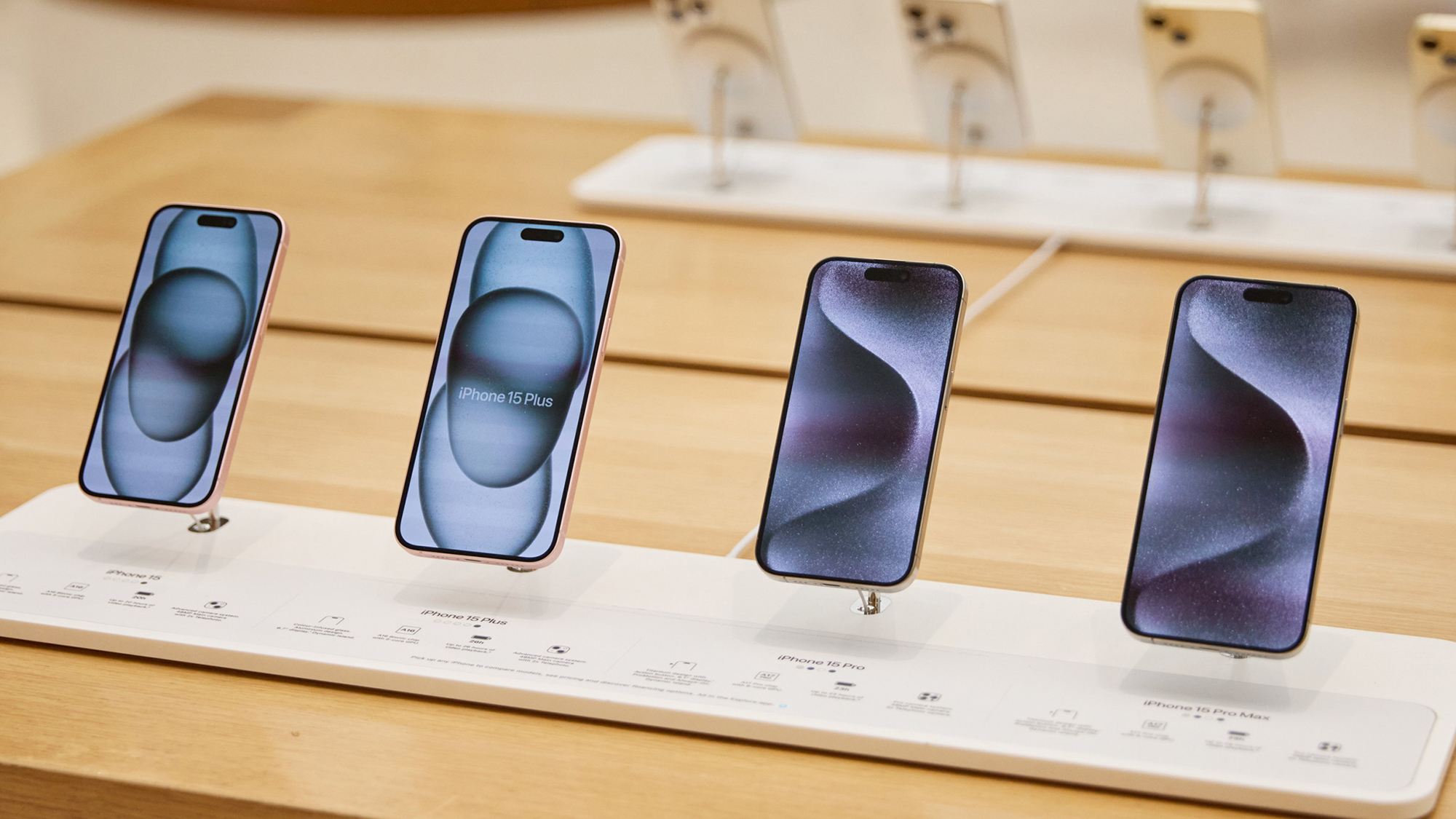
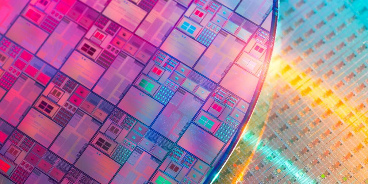
iPhone 18 Pro, iPhone Fold to Feature New A20 Chip With Advanced WMCM Packaging [Report]
A new investor note from GF Securities analyst Jeff Pu suggests Apple's upcoming iPhone 18 series, which is expected to include foldable models, will use TSMC's next-generation N2 process technology alongside a new Wafer-Level Multi-Chip Module (WMCM) packaging for its A20 chips. This would mean some significant advancements in chip integration and performance for future Apple devices.Pu's report indicates that the A20 chip, slated for the iPhone 18 Fold, iPhone 18 Pro Max, and iPhone 18 Pro, will be manufactured using TSMC's N2 process. This aligns with TSMC's recent updates; the company unveiled its A14 1.4nm process for 2028 and noted at that time that its N2 process was on track to begin volume production later this year.A key development Pu highlighted is the adoption of WMCM packaging for the A20. With this tech, different chip components like the main SoC and DRAM are essentially built together directly on the wafer before being separated. It's said to use something called Redistributed Layer (RDL) technology instead of a typical interposer, which should help with signal quality and keeping things cool.Continue ReadingShare Article:Facebook, Twitter, LinkedIn, Reddit, EmailFollow iClarified:Facebook, Twitter, LinkedIn, Newsletter, App Store, YouTube
![iPhone 18 Pro, iPhone Fold to Feature New A20 Chip With Advanced WMCM Packaging [Report]](https://www.iclarified.com/images/news/97494/97494/97494-1280.jpg)
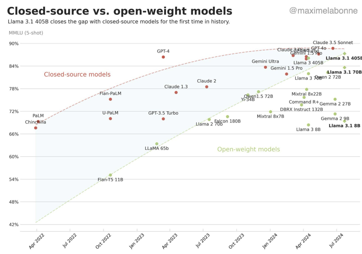
A new investor note from GF Securities analyst Jeff Pu suggests Apple's upcoming iPhone 18 series, which is expected to include foldable models, will use TSMC's next-generation N2 process technology alongside a new Wafer-Level Multi-Chip Module (WMCM) packaging for its A20 chips. This would mean some significant advancements in chip integration and performance for future Apple devices.
Pu's report indicates that the A20 chip, slated for the iPhone 18 Fold, iPhone 18 Pro Max, and iPhone 18 Pro, will be manufactured using TSMC's N2 process. This aligns with TSMC's recent updates; the company unveiled its A14 1.4nm process for 2028 and noted at that time that its N2 process was on track to begin volume production later this year.
A key development Pu highlighted is the adoption of WMCM packaging for the A20. With this tech, different chip components like the main SoC and DRAM are essentially built together directly on the wafer before being separated. It's said to use something called Redistributed Layer (RDL) technology instead of a typical interposer, which should help with signal quality and keeping things cool.
Continue Reading
Share Article:
Facebook, Twitter, LinkedIn, Reddit, Email
Follow iClarified:
Facebook, Twitter, LinkedIn, Newsletter, App Store, YouTube

![Amazon Could Beat Apple to Market With Foldable Tablet [Kuo]](https://www.iclarified.com/images/news/97384/97384/97384-640.jpg)
![Apple Releases watchOS 11.5 for Apple Watch [Download]](https://www.iclarified.com/images/news/97304/97304/97304-640.jpg)
