


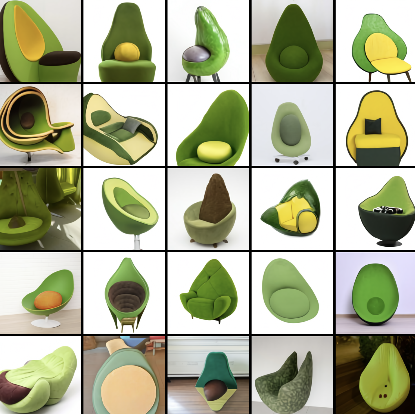


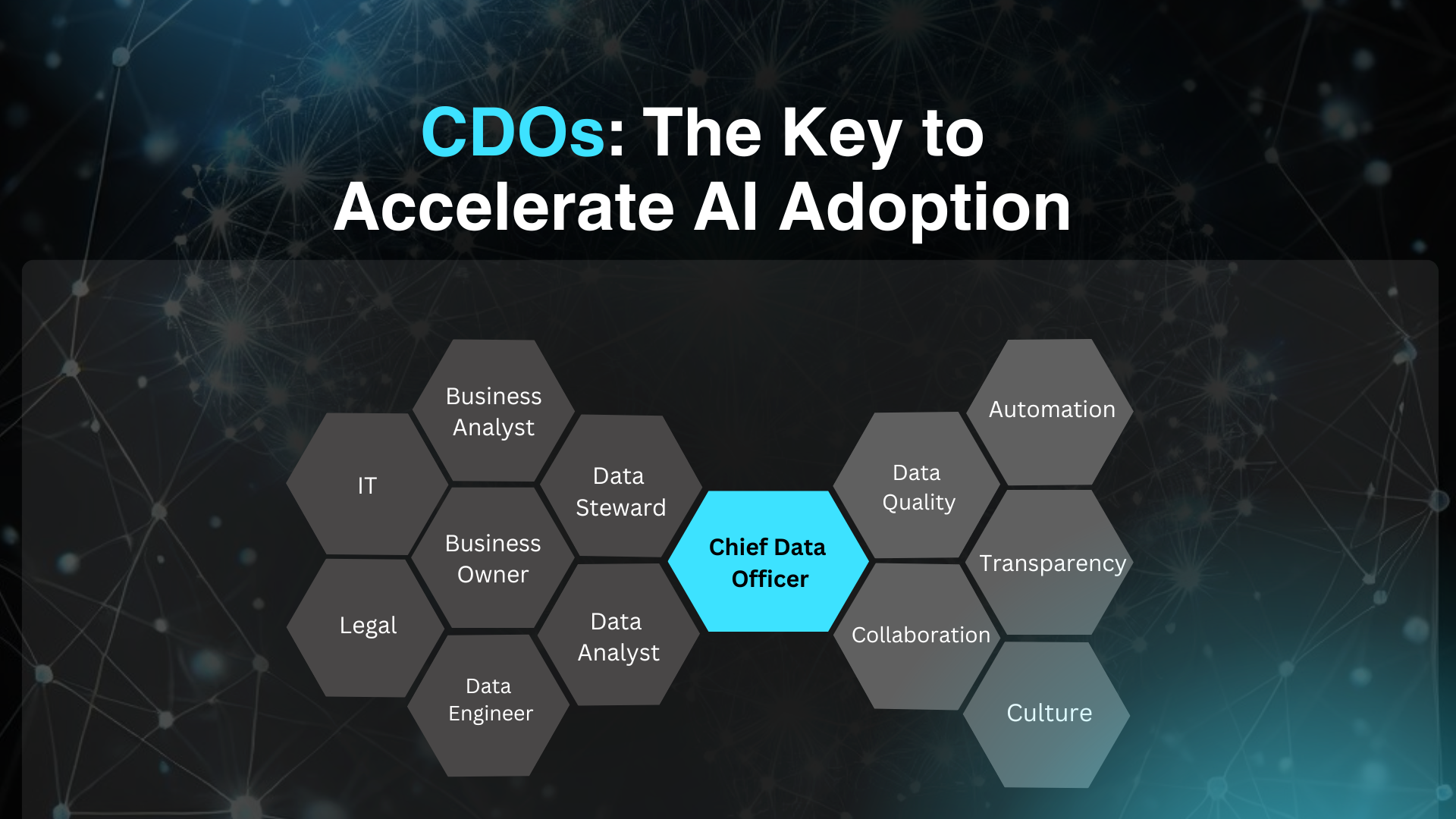
![[The AI Show Episode 146]: Rise of “AI-First” Companies, AI Job Disruption, GPT-4o Update Gets Rolled Back, How Big Consulting Firms Use AI, and Meta AI App](https://www.marketingaiinstitute.com/hubfs/ep%20146%20cover.png)


![Honor 400 series officially launching on May 22 as design is revealed [Video]](https://i0.wp.com/9to5google.com/wp-content/uploads/sites/4/2025/05/honor-400-series-announcement-1.png?resize=1200%2C628&quality=82&strip=all&ssl=1)


![Beats Studio Pro Wireless Headphones Now Just $169.95 - Save 51%! [Deal]](https://www.iclarified.com/images/news/97258/97258/97258-640.jpg)


How to Communicate Between CPLD and FPGA?
Communication between a CPLD (Complex Programmable Logic Device) and an FPGA (Field-Programmable Gate Array) depends on the required speed, complexity, and available I/O resources. Below are common methods, along with their advantages and trade-offs. 1. Parallel Bus (Fast & Simple) Method: Use multiple I/O pins for data transfer (e.g., 8-bit, 16-bit, or 32-bit parallel bus). Add control signals like: CLK (synchronization clock) WR (write enable) RD (read enable) CS (chip select) ACK (acknowledge handshake, if needed). Pros: ✅ High-speed data transfer (good for burst transfers). ✅ Simple to implement (no complex protocols). Cons: ❌ Requires many I/O pins (not ideal for pin-limited designs). ❌ Susceptible to noise (if long traces are used). Example Connection: FPGA (Master) CPLD (Slave) ------------------------- DATA[7:0] DATA[7:0] ADDR[3:0] --------> ADDR[3:0] WR --------> WR RD --------> RD CS --------> CS CLK --------> CLK 2. Serial Communication (Saves Pins) Methods: A. SPI (Serial Peripheral Interface) 4-wire protocol (SCLK, MOSI, MISO, SS). Supports full-duplex communication. Typical speeds: 1–100 MHz. B. I²C (Inter-Integrated Circuit) 2-wire protocol (SCL, SDA). Supports multi-master mode. Slower (~400 kHz – 3.4 MHz). C. UART (Asynchronous Serial) 2-wire (TX, RX) or 1-wire (half-duplex). No clock needed (baud rate must match). Simple but slower (typical speeds: 9600–115200 bps). Pros: ✅ Fewer pins required (good for small CPLDs). ✅ Standardized protocols (easy to interface with MCUs). Cons: ❌ Slower than parallel bus. ❌ SPI/I²C require clock synchronization. Example (SPI Connection): FPGA (Master) CPLD (Slave) ------------------------- SCLK --------> SCLK MOSI --------> SDI MISO CS 3. Dual-Port RAM / FIFO (High-Speed Buffering) Method: Use a shared memory block (if FPGA has embedded RAM). FPGA writes data, CPLD reads (or vice versa). Handshake signals (FULL, EMPTY, WR_EN, RD_EN) synchronize access. Pros: ✅ High throughput (good for streaming data). ✅ Reduces real-time synchronization issues. Cons: ❌ Requires RAM resources (may not be available in small CPLDs). Example (FPGA-to-CPLD FIFO): verilog // FPGA writes data always @(posedge clk) begin if (wr_en && !fifo_full) begin fifo_data RX_P TX_N --------> RX_N 5. Custom Protocol (Flexible but Complex) Method: Define a custom handshake protocol (e.g., source-synchronous). Example: FPGA sends data + strobe signal. CPLD latches data on strobe edge. Pros: ✅ Optimized for specific needs. Cons: ❌ Requires careful timing analysis. Example (Custom Strobe-Based Transfer): verilog // FPGA sends data always @(posedge clk) begin if (send_data) begin data_bus

Communication between a CPLD (Complex Programmable Logic Device) and an FPGA (Field-Programmable Gate Array) depends on the required speed, complexity, and available I/O resources. Below are common methods, along with their advantages and trade-offs.
1. Parallel Bus (Fast & Simple)
Method:
Use multiple I/O pins for data transfer (e.g., 8-bit, 16-bit, or 32-bit parallel bus).
Add control signals like:
- CLK (synchronization clock)
- WR (write enable)
- RD (read enable)
- CS (chip select)
- ACK (acknowledge handshake, if needed).
Pros:
✅ High-speed data transfer (good for burst transfers).
✅ Simple to implement (no complex protocols).
Cons:
❌ Requires many I/O pins (not ideal for pin-limited designs).
❌ Susceptible to noise (if long traces are used).
Example Connection:
FPGA (Master)          CPLD (Slave)
-------------------------
DATA[7:0]  <------->  DATA[7:0]
ADDR[3:0]  -------->  ADDR[3:0]
WR         -------->  WR
RD         -------->  RD
CS         -------->  CS
CLK        -------->  CLK
2. Serial Communication (Saves Pins)
Methods:
A. SPI (Serial Peripheral Interface)
- 4-wire protocol (SCLK, MOSI, MISO, SS).
- Supports full-duplex communication.
- Typical speeds: 1–100 MHz.
B. I²C (Inter-Integrated Circuit)
- 2-wire protocol (SCL, SDA).
- Supports multi-master mode.
- Slower (~400 kHz – 3.4 MHz).
C. UART (Asynchronous Serial)
- 2-wire (TX, RX) or 1-wire (half-duplex).
- No clock needed (baud rate must match).
- Simple but slower (typical speeds: 9600–115200 bps).
Pros:
✅ Fewer pins required (good for small CPLDs).
✅ Standardized protocols (easy to interface with MCUs).
Cons:
❌ Slower than parallel bus.
❌ SPI/I²C require clock synchronization.
Example (SPI Connection):
FPGA (Master)          CPLD (Slave)
-------------------------
SCLK       -------->  SCLK
MOSI       -------->  SDI
MISO       <-------  SDO
SS         -------->  CS
3. Dual-Port RAM / FIFO (High-Speed Buffering)
Method:
- Use a shared memory block (if FPGA has embedded RAM).
- FPGA writes data, CPLD reads (or vice versa).
- Handshake signals (FULL, EMPTY, WR_EN, RD_EN) synchronize access.
Pros:
✅ High throughput (good for streaming data).
✅ Reduces real-time synchronization issues.
Cons:
❌ Requires RAM resources (may not be available in small CPLDs).
Example (FPGA-to-CPLD FIFO):
verilog
// FPGA writes data
always @(posedge clk) begin
    if (wr_en && !fifo_full) begin
        fifo_data <= data_to_send;
    end
end

// CPLD reads data
always @(posedge clk) begin
    if (rd_en && !fifo_empty) begin
        received_data <= fifo_data;
    end
end
4. LVDS / Differential Signaling (Noise Immunity)
Method:
- Use LVDS (Low-Voltage Differential Signaling) for high-speed serial links.
- Example: Xilinx SelectIO, Intel LVDS.
- Requires serializer/deserializer (SerDes) if using high speeds (>1 Gbps).
Pros:
✅ High-speed & noise-resistant (good for long PCB traces).
✅ Fewer pins than parallel bus.
Cons:
❌ More complex to implement.
❌ CPLD may not support LVDS (check datasheet).
Example (LVDS Connection):
FPGA (TX)          CPLD (RX)
-------------------------
TX_P       -------->  RX_P
TX_N       -------->  RX_N
5. Custom Protocol (Flexible but Complex)
Method:
Define a custom handshake protocol (e.g., source-synchronous).
Example:
- FPGA sends data + strobe signal.
- CPLD latches data on strobe edge.
Pros:
✅ Optimized for specific needs.
Cons:
❌ Requires careful timing analysis.
Example (Custom Strobe-Based Transfer):
verilog
// FPGA sends data
always @(posedge clk) begin
    if (send_data) begin
        data_bus <= data;
        strobe <= ~strobe; // Toggle strobe
    end
end

// CPLD receives data
always @(posedge strobe) begin
    received_data <= data_bus;
end
Comparison of Methods

How to Choose?
- Need high speed? → Parallel bus or LVDS.
- Limited pins? → SPI, I²C, or UART.
- Buffered data transfer? → Dual-port RAM/FIFO.
- Noise immunity needed? → LVDS.