


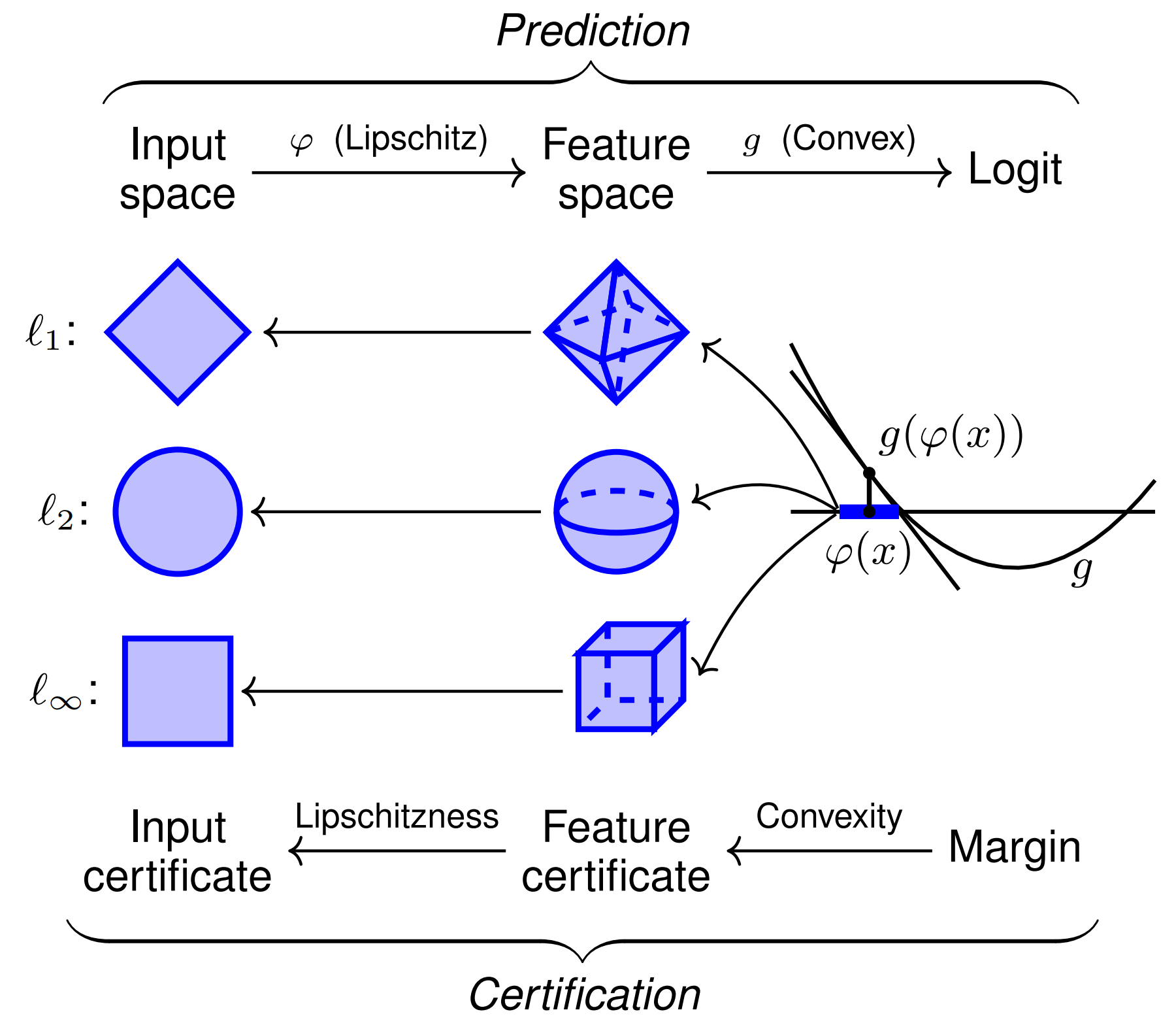
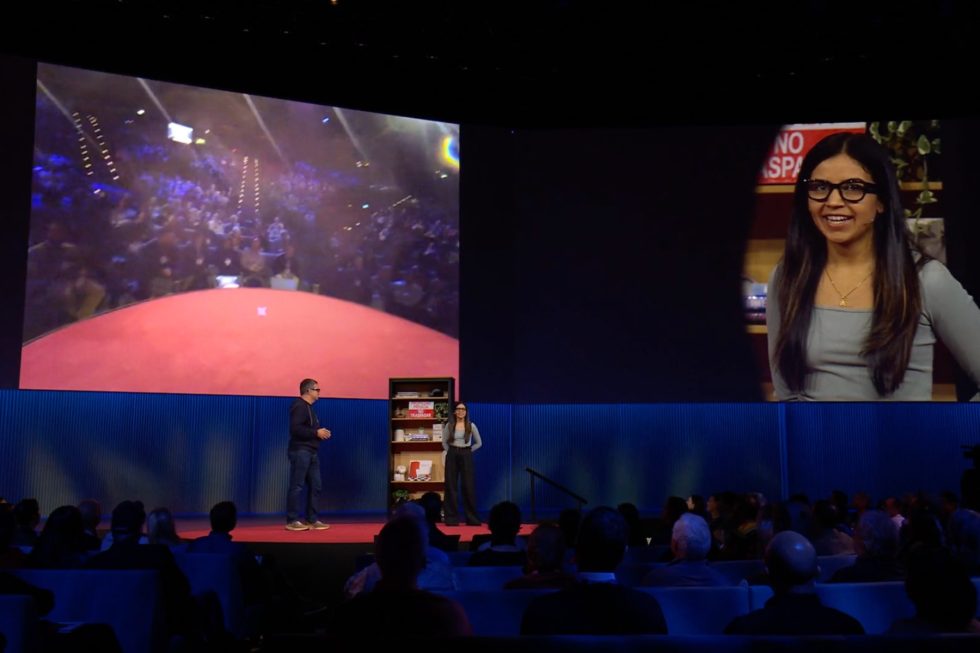
![[The AI Show Episode 144]: ChatGPT’s New Memory, Shopify CEO’s Leaked “AI First” Memo, Google Cloud Next Releases, o3 and o4-mini Coming Soon & Llama 4’s Rocky Launch](https://www.marketingaiinstitute.com/hubfs/ep%20144%20cover.png)


![Is this too much for a modular monolith system? [closed]](https://i.sstatic.net/pYL1nsfg.png)


_Andreas_Prott_Alamy.jpg?width=1280&auto=webp&quality=80&disable=upscale#)


![What features do you get with Gemini Advanced? [April 2025]](https://i0.wp.com/9to5google.com/wp-content/uploads/sites/4/2024/02/gemini-advanced-cover.jpg?resize=1200%2C628&quality=82&strip=all&ssl=1)


![Apple Shares Official Trailer for 'Long Way Home' Starring Ewan McGregor and Charley Boorman [Video]](https://www.iclarified.com/images/news/97069/97069/97069-640.jpg)
![Apple Watch Series 10 Back On Sale for $299! [Lowest Price Ever]](https://www.iclarified.com/images/news/96657/96657/96657-640.jpg)
![EU Postpones Apple App Store Fines Amid Tariff Negotiations [Report]](https://www.iclarified.com/images/news/97068/97068/97068-640.jpg)
![Apple Slips to Fifth in China's Smartphone Market with 9% Decline [Report]](https://www.iclarified.com/images/news/97065/97065/97065-640.jpg)


4K HDMI 2.0 on Artix-7
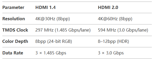
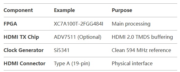
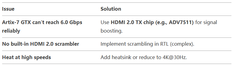
Implementing 4K HDMI 2.0 (2160p@30Hz or 1080p@60Hz) on a Xilinx Artix-7 FPGA is challenging but feasible with careful design. Below is a structured guide covering hardware, IP cores, timing, and debugging. 1. 4K HDMI 2.0 Requirements Artix-7 Limitation: Most Artix-7 FPGAs (e.g., XC7A35T, XC7A100T) support up to 6.6 Gbps per GTX lane, making 4K@30Hz (3 × 1.485 Gbps) achievable, but 4K@60Hz (3 × 3.0 Gbps) is borderline (requires high-speed-grade FPGAs). 2. Hardware Setup Required Components Schematic Considerations TMDS Differential Pairs Route as 100Ω impedance-matched traces (length-matched ±50 mils). Use FPGA bank 34/35 (HP banks for better signal integrity). Power Supply 3.3V for HDMI DDC/HPD. 1.2V for GTX transceivers. 3. FPGA Implementation Steps A. Video Processing Pipeline Input Source Test pattern generator (e.g., color bars) or camera input (MIPI CSI-2 → FPGA). Pixel Clock: 148.5 MHz (for 4K@30Hz). Color Space Conversion Convert YUV → RGB if needed (matrix multiplication in RTL). Timing Control Generate HSYNC, VSYNC, DE signals for HDMI timing. B. TMDS Encoding (8b/10b) verilog module tmds_encoder ( input clk_pixel, input [7:0] data, input [1:0] ctrl, // HSYNC, VSYNC output reg [9:0] tmds ); // 8b/10b encoding logic here // Minimize transitions using XOR/XNOR endmodule C. High-Speed Serialization (GTX) Use Xilinx GTX transceivers (Artix-7 supports up to 6.6 Gbps). Configure 1:10 serialization (594 MHz → 5.94 Gbps per lane). Xilinx IP Core Setup: GTXE2_CHANNEL primitive for TMDS lanes. TXOUTCLK for pixel clock recovery. D. HDMI 2.0 Compliance Scrambling (required for HDMI 2.0 > 3.4 Gbps). DDC/EDID (I²C slave for display handshake). 4. Example Vivado Workflow Step 1: Configure GTX Transceiver tcl create_ip -name gtwizard -vendor xilinx.com -library ip -version 3.6 \ -module_name hdmi_gtx set_property CONFIG.CHANNEL_ENABLE {0 1 2} [get_ips hdmi_gtx] # 3 data lanes set_property CONFIG.LINE_RATE {5.94} [get_ips hdmi_gtx] # 5.94 Gbps Step 2: Generate TMDS Clock tcl create_ip -name clk_wiz -vendor xilinx.com -library ip -version 6.0 \ -module_name hdmi_clk set_property CONFIG.CLKOUT2_REQUESTED_OUT_FREQ {594} [get_ips hdmi_clk] # TMDS bit clock Step 3: Assign FPGA Pins tcl set_property PACKAGE_PIN G12 [get_ports HDMI_TX_P[0]] # Lane 0 (Diff pair) set_property IOSTANDARD TMDS_33 [get_ports HDMI_TX_P*] 5. Debugging Tips Test Pattern First Verify HDMI output with static color bars before real video. Signal Integrity Checks Use a high-speed oscilloscope (≥1 GHz) to inspect TMDS eye diagrams. EDID Emulation Force 4K resolution if the display doesn’t handshake. 6. Limitations & Workarounds 7. Open-Source Projects for Reference FPGA HDMI 2.0 Core (Lattice ECP5): GitHub: hdmi2.0-fpga Xilinx GTX Example: Xilinx PG168 Conclusion 4K@30Hz is achievable on Artix-7 with GTX transceivers. 4K@60Hz is borderline (requires ADV7511 or Kintex-7). Critical steps: TMDS encoding, GTX serialization, signal integrity.
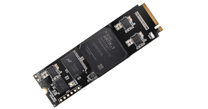
Implementing 4K HDMI 2.0 (2160p@30Hz or 1080p@60Hz) on a Xilinx Artix-7 FPGA is challenging but feasible with careful design. Below is a structured guide covering hardware, IP cores, timing, and debugging.
1. 4K HDMI 2.0 Requirements
Artix-7 Limitation:
Most Artix-7 FPGAs (e.g., XC7A35T, XC7A100T) support up to 6.6 Gbps per GTX lane, making 4K@30Hz (3 × 1.485 Gbps) achievable, but 4K@60Hz (3 × 3.0 Gbps) is borderline (requires high-speed-grade FPGAs).
2. Hardware Setup
Required Components
Schematic Considerations
- TMDS Differential Pairs
- Route as 100Ω impedance-matched traces (length-matched ±50 mils).
- Use FPGA bank 34/35 (HP banks for better signal integrity).
- Power Supply
- 3.3V for HDMI DDC/HPD.
- 1.2V for GTX transceivers.
3. FPGA Implementation Steps
A. Video Processing Pipeline
- Input Source
- Test pattern generator (e.g., color bars) or camera input (MIPI CSI-2 → FPGA).
- Pixel Clock: 148.5 MHz (for 4K@30Hz).
- Color Space Conversion
Convert YUV → RGB if needed (matrix multiplication in RTL).
- Timing Control
Generate HSYNC, VSYNC, DE signals for HDMI timing.
B. TMDS Encoding (8b/10b)
verilog

module tmds_encoder (
    input clk_pixel,
    input [7:0] data,
    input [1:0] ctrl,  // HSYNC, VSYNC
    output reg [9:0] tmds
);
    // 8b/10b encoding logic here
    // Minimize transitions using XOR/XNOR
endmodule
C. High-Speed Serialization (GTX)
- Use Xilinx GTX transceivers (Artix-7 supports up to 6.6 Gbps).
- Configure 1:10 serialization (594 MHz → 5.94 Gbps per lane).
Xilinx IP Core Setup:
- GTXE2_CHANNEL primitive for TMDS lanes.
- TXOUTCLK for pixel clock recovery.
D. HDMI 2.0 Compliance
- Scrambling (required for HDMI 2.0 > 3.4 Gbps).
- DDC/EDID (I²C slave for display handshake).
4. Example Vivado Workflow
Step 1: Configure GTX Transceiver
tcl

create_ip -name gtwizard -vendor xilinx.com -library ip -version 3.6 \
          -module_name hdmi_gtx
set_property CONFIG.CHANNEL_ENABLE {0 1 2} [get_ips hdmi_gtx]  # 3 data lanes
set_property CONFIG.LINE_RATE {5.94} [get_ips hdmi_gtx]        # 5.94 Gbps
Step 2: Generate TMDS Clock
tcl

create_ip -name clk_wiz -vendor xilinx.com -library ip -version 6.0 \
          -module_name hdmi_clk
set_property CONFIG.CLKOUT2_REQUESTED_OUT_FREQ {594} [get_ips hdmi_clk]  # TMDS bit clock
Step 3: Assign FPGA Pins
tcl

set_property PACKAGE_PIN G12 [get_ports HDMI_TX_P[0]]  # Lane 0 (Diff pair)
set_property IOSTANDARD TMDS_33 [get_ports HDMI_TX_P*]
5. Debugging Tips
- Test Pattern First
Verify HDMI output with static color bars before real video.
- Signal Integrity Checks
Use a high-speed oscilloscope (≥1 GHz) to inspect TMDS eye diagrams.
- EDID Emulation
Force 4K resolution if the display doesn’t handshake.
6. Limitations & Workarounds
7. Open-Source Projects for Reference
- FPGA HDMI 2.0 Core (Lattice ECP5):
GitHub: hdmi2.0-fpga
- Xilinx GTX Example:
Xilinx PG168
Conclusion
- 4K@30Hz is achievable on Artix-7 with GTX transceivers.
- 4K@60Hz is borderline (requires ADV7511 or Kintex-7).
- Critical steps: TMDS encoding, GTX serialization, signal integrity.

![[Part 2]TypeScript Fundamentals – Syntax, Data Types, and Operators for QA](https://media2.dev.to/dynamic/image/width=800%2Cheight=%2Cfit=scale-down%2Cgravity=auto%2Cformat=auto/https%3A%2F%2Fdev-to-uploads.s3.amazonaws.com%2Fuploads%2Farticles%2Ft8kbjtr43le4x9cer1rn.png)
