


![[The AI Show Episode 143]: ChatGPT Revenue Surge, New AGI Timelines, Amazon’s AI Agent, Claude for Education, Model Context Protocol & LLMs Pass the Turing Test](https://www.marketingaiinstitute.com/hubfs/ep%20143%20cover.png)


_NicoElNino_Alamy.jpg?width=1280&auto=webp&quality=80&disable=upscale#)

_roibu_Alamy.jpg?width=1280&auto=webp&quality=80&disable=upscale#)


![M4 MacBook Air Drops to Just $849 - Act Fast! [Lowest Price Ever]](https://www.iclarified.com/images/news/97140/97140/97140-640.jpg)
![Apple Smart Glasses Not Close to Being Ready as Meta Targets 2025 [Gurman]](https://www.iclarified.com/images/news/97139/97139/97139-640.jpg)
![iPadOS 19 May Introduce Menu Bar, iOS 19 to Support External Displays [Rumor]](https://www.iclarified.com/images/news/97137/97137/97137-640.jpg)


FPGA Clock Design Scheme: Best Practices and Implementation Guide
Clock design is critical for FPGA systems to ensure timing closure, low jitter, and high reliability. This guide covers clock architecture, PLL/DCM usage, clock domain crossing (CDC), and advanced techniques for Xilinx, Intel (Altera), and Lattice FPGAs. 1. FPGA Clocking Fundamentals Key Concepts FPGA Clock Resources 2. Clock Network Architecture A. Global vs. Regional Clocks Recommendation: Use BUFG (Xilinx) or Global Clock Network (Intel) for critical clocks. Use BUFR/BUFH (Xilinx) for regional clocks. B. Clock Distribution Example (Xilinx 7-Series) [External OSC] → [IBUFG] → [MMCM] → [BUFG] → [CLB/BRAM/DSP] ↘ [BUFH] → [I/O Bank] 3. Generating Clocks with PLL/DCM A. Xilinx MMCM/PLL Configuration verilog // Xilinx Verilog Example MMCME2_BASE #( .CLKIN1_PERIOD(10.0), // 100 MHz input .CLKFBOUT_MULT_F(10), // 1 GHz VCO .CLKOUT0_DIVIDE(10), // 100 MHz output .CLKOUT1_DIVIDE(20) // 50 MHz output ) mmcm_inst ( .CLKIN1(clk_100m), .CLKFBIN(fb_clk), .CLKOUT0(clk_100m_out), .CLKOUT1(clk_50m_out), .LOCKED(mmcm_locked) ); B. Intel FPGA PLL (Quartus) verilog // Intel PLL Example pll_100m pll_inst ( .refclk(clk_50m), // 50 MHz input .rst(reset), .outclk_0(clk_100m), // 100 MHz output .locked(pll_locked) ); C. Key Parameters 4. Clock Domain Crossing (CDC) Techniques When signals cross clock domains, synchronizers prevent metastability. A. Basic 2-Stage Synchronizer verilog // Verilog CDC Example reg [1:0] sync_reg; always @(posedge clk_dest) begin sync_reg
Clock design is critical for FPGA systems to ensure timing closure, low jitter, and high reliability. This guide covers clock architecture, PLL/DCM usage, clock domain crossing (CDC), and advanced techniques for Xilinx, Intel (Altera), and Lattice FPGAs.
1. FPGA Clocking Fundamentals
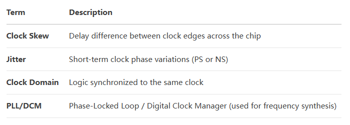
Key Concepts
FPGA Clock Resources
2. Clock Network Architecture
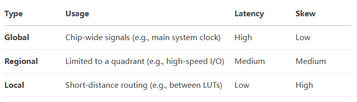
A. Global vs. Regional Clocks
Recommendation:
- Use BUFG (Xilinx) or Global Clock Network (Intel) for critical clocks.
- Use BUFR/BUFH (Xilinx) for regional clocks.
B. Clock Distribution Example (Xilinx 7-Series)
[External OSC] → [IBUFG] → [MMCM] → [BUFG] → [CLB/BRAM/DSP]
                          ↘ [BUFH] → [I/O Bank]
3. Generating Clocks with PLL/DCM
A. Xilinx MMCM/PLL Configuration
verilog
// Xilinx Verilog Example
MMCME2_BASE #(
  .CLKIN1_PERIOD(10.0),    // 100 MHz input
  .CLKFBOUT_MULT_F(10),    // 1 GHz VCO
  .CLKOUT0_DIVIDE(10),     // 100 MHz output
  .CLKOUT1_DIVIDE(20)      // 50 MHz output
) mmcm_inst (
  .CLKIN1(clk_100m),
  .CLKFBIN(fb_clk),
  .CLKOUT0(clk_100m_out),
  .CLKOUT1(clk_50m_out),
  .LOCKED(mmcm_locked)
);
B. Intel FPGA PLL (Quartus)
verilog
// Intel PLL Example
pll_100m pll_inst (
  .refclk(clk_50m),     // 50 MHz input
  .rst(reset),
  .outclk_0(clk_100m),  // 100 MHz output
  .locked(pll_locked)
);
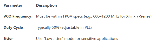
C. Key Parameters
4. Clock Domain Crossing (CDC) Techniques
When signals cross clock domains, synchronizers prevent metastability.
A. Basic 2-Stage Synchronizer
verilog
// Verilog CDC Example
reg [1:0] sync_reg;
always @(posedge clk_dest) begin
  sync_reg <= {sync_reg[0], async_signal};
end
assign sync_signal = sync_reg[1];
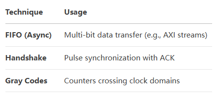
B. Advanced CDC Methods
C. Xilinx Constraints for CDC
tcl
# XDC Constraint
set_false_path -from [get_clocks clk_a] -to [get_clocks clk_b]
5. Low-Jitter Clock Design
A. Reducing Jitter
- Use Dedicated Clock Input Pins (Avoid general-purpose I/O)
- Enable PLL "Low Jitter" Mode
- Minimize Switching Noise (Separate analog/digital power)
B. Jitter Measurement
- Tools: Tektronix Oscilloscope (Eye Diagram)
- FPGA IP: Xilinx IBERT, Intel Signal Tap
6. Dynamic Clock Switching
A. Xilinx BUFGCTRL
verilog
BUFGCTRL bufg_switch (
  .I0(clk_100m),
  .I1(clk_50m),
  .S0(select_100m),
  .S1(select_50m),
  .O(clk_out)
);
B. Glitch-Free Switching
- Use "Clock Mux" IP (Xilinx CLKGEN)
- Ensure no overlap during switching
7. Debugging Clock Issues
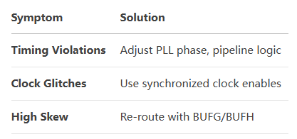
Tools:
- Xilinx: Timing Analyzer, Clocking Wizard
- Intel: TimeQuest, SignalTap
- Lattice: Reveal Logic Analyzer
8. Advanced Techniques
A. Sub-Clocking (Clock Enables)
verilog
// Generate 25 MHz from 100 MHz using CE
reg [1:0] ce_counter;
always @(posedge clk_100m) begin
  ce_counter <= ce_counter + 1;
end
assign clk_25m_enable = (ce_counter == 0);
B. SerDes Clocking (High-Speed I/O)
- Use ISERDES/OSERDES (Xilinx) or LVDS I/O (Intel)
- Example: DDR data capture at 800 Mbps
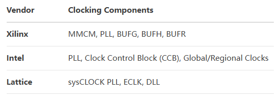
9. Vendor-Specific Recommendations
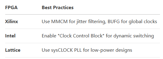
Conclusion
- Use global clocks for critical paths.
- Synchronize CDC with FIFOs or handshakes.
- Minimize jitter with PLL tuning.
- Verify timing with vendor tools.