


![[The AI Show Episode 143]: ChatGPT Revenue Surge, New AGI Timelines, Amazon’s AI Agent, Claude for Education, Model Context Protocol & LLMs Pass the Turing Test](https://www.marketingaiinstitute.com/hubfs/ep%20143%20cover.png)


![Is this too much for a modular monolith system? [closed]](https://i.sstatic.net/pYL1nsfg.png)


-The-Elder-Scrolls-IV-Oblivion-Remastered---Official-Reveal-00-18-14.png?width=1920&height=1920&fit=bounds&quality=70&format=jpg&auto=webp#)


_roibu_Alamy.jpg?width=1280&auto=webp&quality=80&disable=upscale#)


 CISO’s Core Focus.webp?#)


![Apple Smart Glasses Not Close to Being Ready as Meta Targets 2025 [Gurman]](https://www.iclarified.com/images/news/97139/97139/97139-640.jpg)
![iPadOS 19 May Introduce Menu Bar, iOS 19 to Support External Displays [Rumor]](https://www.iclarified.com/images/news/97137/97137/97137-640.jpg)

![Apple Drops New Immersive Adventure Episode for Vision Pro: 'Hill Climb' [Video]](https://www.iclarified.com/images/news/97133/97133/97133-640.jpg)


How to use Xilinx FPGA differential input clock?
Differential clocks provide superior noise immunity and signal integrity compared to single-ended clocks, especially for high-frequency designs. Here's how to properly implement them in Xilinx FPGAs: 1. Hardware Connections Supported Standards: LVDS (Low Voltage Differential Signaling) LVDS_25 (2.5V variant) LVPECL (via AC coupling) HSTL (High-Speed Transceiver Logic) Differential HSTL/SSTL for memory interfaces Board-Level Connection Example: FPGA Board: DIFF_CLK_P ----+ |---- Xilinx FPGA MRCC/SRCC clock-capable pin pair DIFF_CLK_N ----+ 2. Xilinx Clock Resources Clock-Capable Pins: MRCC (Multi-Region Clock Capable) SRCC (Single-Region Clock Capable) HRCC (High-Range Clock Capable in UltraScale+) Locating Pins: Consult your device's "SelectIO Resources" user guide In Vivado: Tools → Language Templates → HDL → Verilog/VHDL → IO → Differential Inputs 3. Implementation Methods A. Using IBUFDS (Verilog) verilog // Differential input buffer for clocks IBUFDS #( .DIFF_TERM("TRUE"), // Enable differential termination .IBUF_LOW_PWR("FALSE") // High performance mode ) ibufds_inst ( .I(clk_p), // Differential positive input .IB(clk_n), // Differential negative input .O(clk_out) // Single-ended clock output ); B. Using IBUFGDS for Global Clock Buffers verilog // For clock inputs that will drive global clock networks IBUFGDS #( .DIFF_TERM("TRUE") ) ibufgds_inst ( .I(sys_clk_p), .IB(sys_clk_n), .O(sys_clk) ); C. VHDL Implementation vhdl library UNISIM; use UNISIM.VCOMPONENTS.ALL; entity clk_input is port( clk_p : in std_logic; clk_n : in std_logic; clk_out : out std_logic ); end entity; architecture rtl of clk_input is begin ibufds_inst : IBUFDS generic map ( DIFF_TERM => TRUE, IBUF_LOW_PWR => FALSE ) port map ( I => clk_p, IB => clk_n, O => clk_out ); end architecture; 4. Constraints File (.xdc) Pin Assignment: set_property PACKAGE_PIN AD12 [get_ports clk_p] set_property PACKAGE_PIN AD11 [get_ports clk_n] set_property IOSTANDARD LVDS [get_ports {clk_p clk_n}] Clock Definition: create_clock -name sys_clk -period 5.000 [get_ports clk_p] 5. UltraScale/UltraScale+ Specifics For newer devices, use: verilog IBUFDS_GTE3 #( .REFCLK_EN_TX_PATH(1'b0), .REFCLK_HROW_CK_SEL(2'b00), .REFCLK_ICNTL_RX(2'b00) ) ibufds_gte3_inst ( .I(clk_p), .IB(clk_n), .CEB(1'b0), .O(clk_out) ); 6. Best Practices Termination: Enable internal differential termination (DIFF_TERM="TRUE") when board doesn't have external termination Typical impedance: 100Ω between differential pairs PCB Layout: Keep trace lengths matched (±50ps) Route as differential pair with controlled impedance Minimize vias on clock traces Clock Management: Connect to MMCM/PLL for frequency synthesis Example MMCM connection: verilog MMCME2_BASE #( .CLKIN1_PERIOD(5.0), .CLKFBOUT_MULT_F(10), .CLKOUT0_DIVIDE_F(5) ) mmcm_inst ( .CLKIN1(clk_out), .CLKOUT0(system_clk), // Other connections... ); Simulation: Simulate clock transitions with proper delays: verilog initial begin clk_p = 1'b0; clk_n = 1'b1; forever #2.5 begin clk_p = ~clk_p; clk_n = ~clk_n; end end 7. Debugging Tips Clock Verification: Use ILA (Integrated Logic Analyzer) to verify clock integrity Check for duty cycle distortion Timing Constraints: Set input delay constraints: set_input_delay -clock [get_clocks sys_clk] -max 1.5 [get_ports clk_p] Power Considerations: Monitor clock power consumption in Vivado Power Analysis Consider using BUFGCE for clock gating Common Pitfalls to Avoid Incorrect Standard: Using LVDS_25 when board provides 1.8V signals Missing Termination: Forgetting to enable DIFF_TERM when needed Clock Domain Crossing: Not properly synchronizing signals between differential clock domains Pin Mismatch: Using non-clock-capable pins for high-speed differential clocks By following these guidelines, you can reliably implement differential clock inputs in your Xilinx FPGA designs, ensuring optimal signal integrity and timing performance.
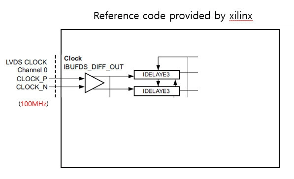
Differential clocks provide superior noise immunity and signal integrity compared to single-ended clocks, especially for high-frequency designs. Here's how to properly implement them in Xilinx FPGAs:
1. Hardware Connections
Supported Standards:
- LVDS (Low Voltage Differential Signaling)
- LVDS_25 (2.5V variant)
- LVPECL (via AC coupling)
- HSTL (High-Speed Transceiver Logic)
- Differential HSTL/SSTL for memory interfaces
Board-Level Connection Example:
FPGA Board:
DIFF_CLK_P  ----+
                |---- Xilinx FPGA MRCC/SRCC clock-capable pin pair
DIFF_CLK_N  ----+
2. Xilinx Clock Resources
Clock-Capable Pins:
- MRCC (Multi-Region Clock Capable)
- SRCC (Single-Region Clock Capable)
- HRCC (High-Range Clock Capable in UltraScale+)
Locating Pins:
- Consult your device's "SelectIO Resources" user guide
- In Vivado: Tools → Language Templates → HDL → Verilog/VHDL → IO → Differential Inputs
3. Implementation Methods
A. Using IBUFDS (Verilog)
verilog
// Differential input buffer for clocks
IBUFDS #(
    .DIFF_TERM("TRUE"),    // Enable differential termination
    .IBUF_LOW_PWR("FALSE") // High performance mode
) ibufds_inst (
    .I(clk_p),    // Differential positive input
    .IB(clk_n),   // Differential negative input
    .O(clk_out)   // Single-ended clock output
);
B. Using IBUFGDS for Global Clock Buffers
verilog
// For clock inputs that will drive global clock networks
IBUFGDS #(
    .DIFF_TERM("TRUE")
) ibufgds_inst (
    .I(sys_clk_p),
    .IB(sys_clk_n),
    .O(sys_clk)
);
C. VHDL Implementation
vhdl
library UNISIM;
use UNISIM.VCOMPONENTS.ALL;

entity clk_input is
port(
    clk_p : in std_logic;
    clk_n : in std_logic;
    clk_out : out std_logic
);
end entity;

architecture rtl of clk_input is
begin
    ibufds_inst : IBUFDS
    generic map (
        DIFF_TERM => TRUE,
        IBUF_LOW_PWR => FALSE
    )
    port map (
        I => clk_p,
        IB => clk_n,
        O => clk_out
    );
end architecture;
4. Constraints File (.xdc)
Pin Assignment:
set_property PACKAGE_PIN AD12 [get_ports clk_p]
set_property PACKAGE_PIN AD11 [get_ports clk_n]
set_property IOSTANDARD LVDS [get_ports {clk_p clk_n}]
Clock Definition:
create_clock -name sys_clk -period 5.000 [get_ports clk_p]
5. UltraScale/UltraScale+ Specifics
For newer devices, use:
verilog
IBUFDS_GTE3 #(
    .REFCLK_EN_TX_PATH(1'b0),
    .REFCLK_HROW_CK_SEL(2'b00),
    .REFCLK_ICNTL_RX(2'b00)
) ibufds_gte3_inst (
    .I(clk_p),
    .IB(clk_n),
    .CEB(1'b0),
    .O(clk_out)
);
6. Best Practices
- Termination:
- Enable internal differential termination (DIFF_TERM="TRUE") when board doesn't have external termination
- Typical impedance: 100Ω between differential pairs
- PCB Layout:
- Keep trace lengths matched (±50ps)
- Route as differential pair with controlled impedance
- Minimize vias on clock traces
- Clock Management:
- Connect to MMCM/PLL for frequency synthesis
- Example MMCM connection:
verilog
MMCME2_BASE #(
    .CLKIN1_PERIOD(5.0),
    .CLKFBOUT_MULT_F(10),
    .CLKOUT0_DIVIDE_F(5)
) mmcm_inst (
    .CLKIN1(clk_out),
    .CLKOUT0(system_clk),
    // Other connections...
);
- Simulation:
Simulate clock transitions with proper delays:
verilog
initial begin
    clk_p = 1'b0;
    clk_n = 1'b1;
    forever #2.5 begin
        clk_p = ~clk_p;
        clk_n = ~clk_n;
    end
end
7. Debugging Tips
- Clock Verification:
- Use ILA (Integrated Logic Analyzer) to verify clock integrity
- Check for duty cycle distortion
- Timing Constraints:
Set input delay constraints:
set_input_delay -clock [get_clocks sys_clk] -max 1.5 [get_ports clk_p]
- Power Considerations:
- Monitor clock power consumption in Vivado Power Analysis
- Consider using BUFGCE for clock gating
Common Pitfalls to Avoid
- Incorrect Standard:
Using LVDS_25 when board provides 1.8V signals
- Missing Termination:
Forgetting to enable DIFF_TERM when needed
- Clock Domain Crossing:
Not properly synchronizing signals between differential clock domains
- Pin Mismatch:
Using non-clock-capable pins for high-speed differential clocks
By following these guidelines, you can reliably implement differential clock inputs in your Xilinx FPGA designs, ensuring optimal signal integrity and timing performance.